Advanced Optical Integration Processes for Photonic‐Integrated
This packaging method results in longer connection path distances between PICs and EICs compared to those in monolithic and 3D co-packaging techniques, leading to the generation of
Advancing Co-Packaged and Near-Packaged Optics: Material
Co-Packaged Optics (CPO) and Near-Packaged Optics (NPO) represent the next major inflection in data-center interconnects. By relocating optical engines adjacent to compute ASICs, they...
Two-photon lithography for integrated photonic packaging
Two-photon lithography (TPL), a laser direct-write three-dimensional (3-D) patterning technique with deep subwavelength resolution, has emerged as a promising solution for integrated photonics
Micromirror fabrication for co-packaged optics using 3D nanoimprint
In the CPO module where silicon chips are embedded on the substrate and polymer waveguides are integrated as optical connections, a pair of 3D micromirrors can achieve low-loss
Advanced Optical Integration Processes for
This packaging method results in longer connection path distances between PICs and EICs compared to those in monolithic and 3D co-packaging
Automated, high-throughput photonic packaging
Silicon photonics can enable optical circuits of unprecedented complexity and cost efficiency. It employs lithography to effectively pre-assemble optical devices on wafers fabricated in

Advanced Packaging Evolution: Chiplet and Silicon Photonics-CPO
Today, OSAT (Outsourced Semiconductor Assembly and Test) is driven not only by the packaging demands of advanced node ICs but also by the rise of emerging technologies like Silicon Photonics
Co-Packaged Optics (CPO): Evaluating Different Packaging
Heterogeneous integration is key to co-packaged optics (CPO), enabling the integration of the optical engine (OE)—which includes photonic ICs (PICs) and electronic ICs (EICs)— with
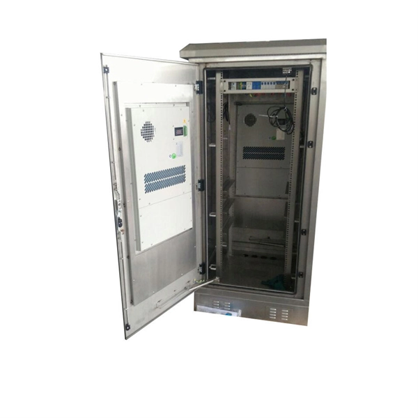
Co-Packaged Optics (CPO) Technology
CPO employs advanced low-temperature fabrication, scalable lithography, and innovative optical packaging to achieve ultra-dense optical I/O with high bandwidth and energy efficiency.
Co-packaged optics (CPO): status, challenges, and solutions
Co-packaged optics (CPO) is a disruptive approach to increasing the interconnecting bandwidth density and energy efficiency by dramatically shortening the electrical link length through
Co-packaging photonics and electronics poses challenges
There are different ways to enhance the integration, such as 3D integration or even monolithic integration where the photonics and electronics exist within the same chip together.”
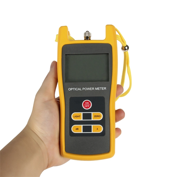
Optical Power Meters & Sources
High-precision power meters (Ge/InGaAs) and stabilized light sources for insertion loss and return loss testing.
OTDR & Fiber Characterization
Full-featured OTDR, fiber OTDR testers, and modular OTDR test modules for network deployment and troubleshooting.
OSA & Eye Diagram Analyzer
High-resolution OSA for DWDM and eye diagram testers for signal integrity validation.
BERT & Endface Inspection
BERT up to 800G, fiber endface inspection probes, and extinction ratio meters for comprehensive testing.