6012_design_project.dvi
Figure 2 shows the schematic of the optical receiver. It consists of three CMOS stages: a tran-simpedance amplifier, a saturating or limiting amplifier, and an output driver.
The Internal Components and Structure of The Optical Transceiver
The optical module is a very important component in an optical communication system. This article will introduce you to the internal components and structure of the optical module.
FTTH Optical Receiver
FTTH Optical Receiver 1. Description TX-1000-A23 FTTH Optical Receiver has high performance, lower receiver optical power and lower cost for CATV operators providing high quality and excellent FTTH
Chapter 9 Optical Receiver Design
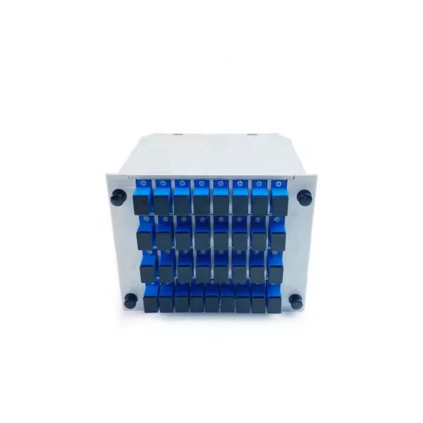
9.2 Receiver optical subassembly (ROSA) consists of an opti-cal detector. The detector is usually part of a rece ver optical subassembly, or ROSA. The role of a ROSA is very much similar to that of a TOSA
Optical module design resources | TI
View the TI Optical module block diagram, product recommendations, reference designs and start designing.
Overview of the Development of Fiber Optic Transceivers
Let''s take the 25G gray optical module as an example to introduce the basic functional block diagram of the optical module. Figure 2 Basic functional block diagram of the optical module.

Design of High-Speed Optical Receiver Module for 160Gb/s NRZ and
In this paper, we propose a high-speed optical receiver module with four channels. The optical receiver module was composed of a four-channel PIN photodiode array and a four-channel linear
Transmitter/receiver photo IC for optical link
Figure 3-1 (b) shows a block diagram of the receiver photo IC. When an optical signal is input to the photodiode, an amplifier converts the current into voltage and amplifies the signal.

Optical Receiver Front-End Integrated Circuit Design
The schematic of the optical receiver front-end circuit is shown in Figure 7.15, where YS is the photodiode (PD) input admittance. Typically this will be that of the PIN/APD and is almost completely

Exploded schematic view of the optical receiver module.
Fig. 2 shows the schematic configuration of the optical receiver module. For cost reduction, we used a novel plastic package, passive alignment using a V-groove substrate, and a Si-bipolar...
Optical Receiver Design
The figure below shows a block diagram of such a receiver. Its components can be arranged into three groups - the front end, the linear channel, and the decision circuit. 1. Front End. The front end of a
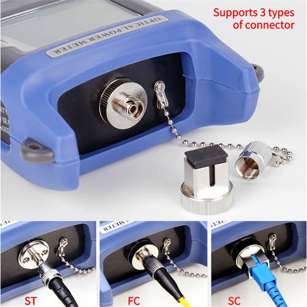
Optical Power Meters & Sources
High-precision power meters (Ge/InGaAs) and stabilized light sources for insertion loss and return loss testing.
OTDR & Fiber Characterization
Full-featured OTDR, fiber OTDR testers, and modular OTDR test modules for network deployment and troubleshooting.
OSA & Eye Diagram Analyzer
High-resolution OSA for DWDM and eye diagram testers for signal integrity validation.
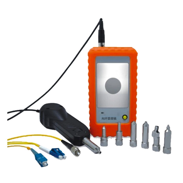
BERT & Endface Inspection
BERT up to 800G, fiber endface inspection probes, and extinction ratio meters for comprehensive testing.